NEWS
Official announcement: Leyard self-developed full-process high-level MIP line Phase I starts mass production!
2024.12.03
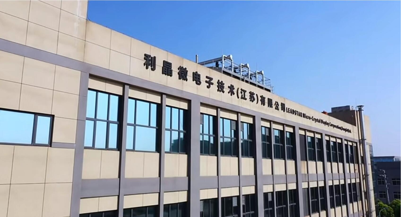
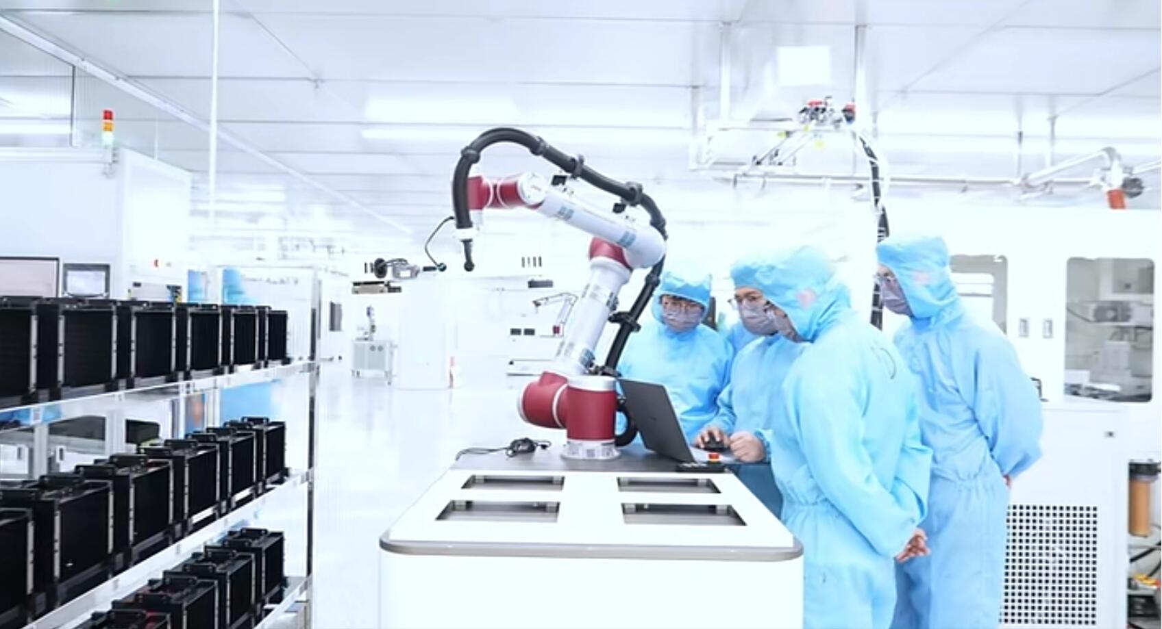
On November 20, 2024, Leyard self-developed full-process high-level MIP line (Micro LED packaging technology) Phase I was officially put into operation at our Leadstar facility in Wuxi, Jiangsu. This will enable the company to keep leading and driving Mirco Led display related technological innovation while accelerating cost reduction, efficiency increase and large-scale application of Micro LED display products.


What is high-level MIP?
• Fully inverted, substrate-free Micro LED chip with a size less than 50μm, an area less than 1/10 of the traditional LED chip, a light-emitting area less than 1% of the screen area, and at least 99% black for a higher contrast ratio;
• The consistent half-power angle of substrate-free RGB LED chip means that the LED screen maintains the consistency of color temperature and chromaticity viewing angle at an angle of 170-degree or larger, providing a perfect solution to color cast.

Benefits of the MIP line
• Efficient automated production: MIP automated bead production line up to Class 1,000 clean room standards that enables automatic and intelligent production. Our self-developed mass transfer and welding technique achieves a transfer efficiency of 6,000kUPH, which is 150 times of an ordinary die bonder, truly reducing costs and increasing efficiency;
• Yield and efficiency higher than the industry average: with mass transfer, mass welding, mass testing, mass cutting, and other key process equipment, Leadstar achieves overall yield and efficiency of key sites in the production process higher than the industry average, with a yield of high-level MIP products > 95%;

The official operation of the MIP line will greatly drive demand for high-definition display with a pixel pitch below 1 mm and bring the market with MicroLED products of higher cost performance and better display effect. It is expected that the capacity of Phase I will reach 1,200KK per month and of Phase II will be expanded to 2,400KK per month.
In order to further reduce the cost of Micro LED and to accelerate its extensive development and adoption, we will keep promoting the mass production and application of glass-based high-level MiP products through cooperation.
Share To
Related Media Reports
2026.03.20
See the World Through Screens | Leyard at ISLE 2026
2025.09.28
Statement on the Adjustment of Leyard Group’s Regional Brand Agency Policy
2025.09.28


-1_1661389830.jpg)